In the world of VLSI, the physical design flow bridges the abstract logic world and the real silicon. In the first two lines, you read “physical design flow” — that’s intentional. This article digs deep into physical design flow, explaining physical design flow in VLSI, pd flow in VLSI, and related topics — from wire length to clock tree synthesis, power planning, and physical verification.
Whether you are a student, a fresh design engineer, or someone polishing up your knowledge, this 4000-word guide will help you master vlsi physical design and all processes inside the design flow.
physical design flow refers to the multi-stage process in VLSI design where a synthesized netlist is transformed into a manufacturable layout. In simpler words, it is the PD flow in VLSI where logical connectivity is converted into actual geometries on silicon — placing standard cells, routing wires, building clock tree synthesis, power planning, verifying rules, and finally handing off to the foundry.
This stage comes after logic synthesis and before tape-out, and is central to achieving the targets of area, timing, power, and yield. Wikipedia+2chipedge.com+2
Before diving into each stage, let’s understand why physical design flow is so key:
In short, physical design flow is where abstract logic is made real — and many design tradeoffs are resolved here.
Before you start the physical design flow in VLSI, you need:
This is the core of the PD process. Each sub-step ensures that the design meets electrical and physical requirements.
Before the actual design flow starts:
Floor planning defines the chip outline, aspect ratio, and macro placement. Partitioning divides the design into manageable blocks.
Power planning ensures stable power distribution across the chip.
Without good power planning, even functional chips can fail due to poor voltage delivery.
Placement arranges standard cells optimally to minimize wire length and congestion.
Post-placement optimization includes:
Reducing congestion hotspots
CTS ensures all sequential elements receive the clock simultaneously.
Steps include:
Routing connects all the placed components electrically.
Good routing minimizes delay, power, and cross-talk while obeying constraints.
Once routing is complete, perform Static Timing Analysis (STA).
Fix violations through:
Achieving timing closure ensures all signals meet setup and hold constraints.
These confirm that the layout is manufacturable and error-free.
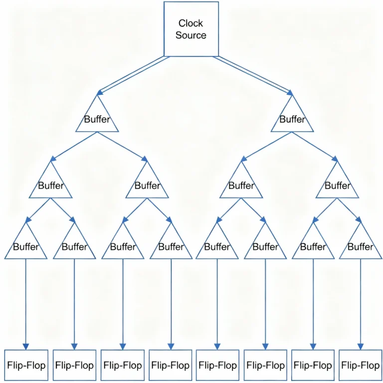
The physical design flow transforms an RTL netlist into a real, manufacturable chip layout. Through steps like floorplanning, placement, clock tree synthesis, routing, and physical verification, engineers ensure high performance, low power, and design compliance