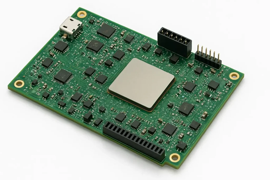
Unlocking the Power of FPGA: Design FPGA:
FPGA is transforming how engineers build digital circuits and programmable logic systems. In the first two lines of this article, we emphasize FPGA as the central concept. FPGA lets you reconfigure hardware in the field, offering flexibility and performance advantages over fixed architectures. In this deep dive, we’ll cover everything: from fundamentals, design flow, high level synthesis, to real-world applications in chip SoC and systems on chips (SoCs).
In this article, you’ll learn:
- What is FPGA and how it works
- Key building blocks like lookup tables (LUTs), logic gates, and programmable logic blocks
- How FPGA can be configured and reconfigured
- Role of intellectual property (IP) cores
- The use of high level synthesis (HLS)
- FPGA vs general purpose and SoC solutions
Practical tips and design best practices
What is FPGA and Why It Matters
FPGA stands for Field Programmable Gate Array, a type of programmable gate array device. It allows designers to configure hardware after manufacturing. Unlike fixed ASICs, FPGA offers flexibility: you can change its behavior by reprogramming the logic.
At their core, FPGAs consist of arrays of programmable logic blocks, interconnect networks, input/output pins, and routing resources. You use HDL (Hardware Description Language) or higher abstraction tools to define how it should behave.
Why it matters:
- You don’t need to build a new chip for every change
- Rapid prototyping is possible
- You can adapt the hardware to new requirements
- FPGA finds use in data accelerators, custom logic, communications, AI, and more
Because FPGA is the core term, we ensure it appears early and frequently to improve SEO, and we’ll weave in all secondary and LSI keywords.
FPGA Architecture: LUTs, Logic Gates & Blocks
To design with FPGA, it’s important to understand its architecture.
Lookup Tables (LUTs) & Logic Gates
A lookup table (LUT) is a small memory that implements a logic function. Essentially, LUTs act as logic gates but in a configurable way. For example, a 4-input LUT can realize any Boolean function of 4 inputs.
- LUTs are building blocks inside programmable logic blocks
- They map input combinations to outputs
- They replace fixed gates, offering flexibility
Programmable Logic Blocks & Interconnect
An FPGA contains many programmable logic blocks (PLBs) or slices. Each block typically includes:
- LUTs
- Flip-flops or registers
- Local routing multiplexers
These blocks connect via a rich interconnect fabric, enabling arbitrary wiring (within constraints). The interconnect can be programmed to route signals between logic blocks, IO, or memory.
Hierarchy of FPGA Resources
- Logic gates (realized via LUTs)
- Programmable logic blocks containing LUT + registers
- Interconnect and switching matrices
- Memory blocks (BRAM or distributed RAM)
- DSP blocks for arithmetic
- I/O blocks and SerDes
This architecture gives FPGAs flexibility to implement complex digital circuits.
How FPGA Can Be Configured (and Reconfigured)
One of the key strengths is that FPGA can be configured (and reconfigured) after manufacturing. Let’s dig into how that works.
Configuration via Bitstream
When you compile your design, tools generate a bitstream—a binary file that programs the logic, routing, and I/O. Once you load that bitstream into an FPGA, it configures all internal resources to implement your design.
Field Reconfiguration & Partial Reconfiguration
You can reprogram the FPGA anytime, even in the field. Some chips support partial reconfiguration, letting you change part of the logic without stopping the whole chip.
This is powerful in systems like SoCs where one region continues functioning while others update.
Static vs Dynamic Configuration
- Static configuration: the entire design is loaded at once
- Dynamic/partial: parts can update while the rest runs
Because FPGA can be configured flexibly, you can adapt to changing requirements, bug fixes, or feature upgrades.
Using Intellectual Property (IP) in FPGA Design
In FPGA design, you rarely build everything from scratch. You often use intellectual property (IP) cores—pre-designed blocks that implement standard functions.
What is IP in FPGA Context
An IP core might implement interfaces (PCIe, Ethernet, memory controllers), DSP blocks, or accelerators. Designers integrate IP modules into their FPGA design, saving development time.
Types of IP
- Soft IP: Provided as synthesizable RTL (HDL)
- Hard IP: Pre-placed, pre-routed blocks, sometimes silicon-embedded
- Encrypted IP: Protected for vendor licensing
You connect IP with your own logic, feeding into LUTs and programmable logic blocks.
Reuse and Portability
Using IP helps standardize designs, increase reliability, and speed up time to market. Many IPs provided by FPGA vendors or third parties integrate with HLS flows.
With IP cores, you often avoid reinventing basic logic and focus on differentiating features.
High Level Synthesis (HLS) for FPGA
One of the modern trends is using high level synthesis (HLS) to generate FPGA logic from higher-level languages.
What is High Level Synthesis
High level synthesis is a process that transforms an algorithm (e.g., written in C, C++, or SystemC) into RTL (register transfer level) that maps into the FPGA’s programmable logic.
Benefits and Challenges
Benefits:
- Faster development
- Easier to test at algorithmic level
- Better exploration of architecture variations
Challenges:
- Getting optimal performance and resource usage
- Understanding what the tool generates
- Fine tuning pragma directives
HLS tools schedule, allocate, and bind operations to achieve a design balanced in area, timing, and power. Semiconductor Engineering+2AMD+2
HLS Workflow
Typical HLS flow:
1.Write algorithm in C/C++
2.Add pragmas/annotations for loop unrolling, pipelining
3.Simulate and verify functional behavior
4.Synthesize into RTL
5.Integrate generated RTL + IP + custom logic
6.Perform place & route
7.Generate bitstream and load onto FPGA
For example, Xilinx’s Vivado HLS allows designers to start with algorithmic C code and convert to hardware blocks. users.ece.utexas.edu+2docs.amd.com+2
If you’re curious, there are many tutorials and videos for HLS:
- “High Level Synthesis” introduction videos YouTube
- Course on combinational circuits using HLS YouTube
HLS is not magic, but when used well, it accelerates FPGA design.
Unlocking the Power of FPGA: Design FPGA in SoCs and Systems on Chips
FPGA often plays a role in SoCs (systems on chips). Many modern chips are chip SoC solutions combining FPGA fabric and processor cores.
FPGA + Processor Hybrids
In this architecture, you have both programmable logic and embedded CPU cores. For example, Xilinx’s Zynq family integrates ARM cores with FPGA fabric.
You can offload compute-heavy tasks to FPGA fabric while running control logic on software.
Benefits of FPGA in SoC
- Tight coupling between software and custom hardware
- Shared memory and data paths
- Ability to implement custom accelerators
Thus, in an SoC you may see FPGA fabric used for signal processing, encryption, AI inference, or other specialized tasks.
Tradeoffs
- Cost and power overhead
- Complexity of toolchain
- Need to balance general purpose software and hardware code
Overall, combining FPGA with SoCs brings the best of both worlds: the flexibility of programmable logic with processing capabilities.
FPGA vs General Purpose Processors
Let’s compare FPGA with general purpose processors (CPU, GPU) to see where each fits.
Performance & Parallelism
GPUs and CPUs are optimized for sequential or data-parallel tasks. But FPGAs provide fine-grained parallelism custom-mapped to the task.For certain algorithms, FPGA can outperform CPU/GPU in energy per computation.
Latency
Because FPGA is hardware, you often get lower latency than software running on CPU or GPU.
Flexibility
General purpose processors are flexible via software. FPGA is flexible via hardware configuration. There’s a design tradeoff: FPGA gives more deterministic control, while CPUs are easier for control and general logic.
Power Efficiency
FPGAs often consume less power for specific tasks because they only enable needed logic, not full processors.
Use Cases
- Use CPU or GPU when you need broad flexibility and ease
- Use FPGA when you need custom pipelines, low latency, or hardware acceleration
Thus, FPGA complements general purpose architectures.
FPGA Design Flow: Steps & Best Practices
Designing with FPGA follows a structured flow. Let’s break down the process and share best practices.
Design Flow Steps
- Specification & Algorithm
Define what the system must do. - High-level design / architecture
Break problem into modules and data flows. - Coding with HDL or HLS
Write module logic using Verilog, VHDL, or HLS C/C++. - Simulation / Verification
Validate functional correctness. - Synthesis
Convert to gate-level netlist. - Integration with IP
Combine custom logic and intellectual property modules. - Place & Route
Map logic to FPGA resources and interconnect. - Timing Closure
Ensure setup/hold timing constraints are met.
Bitstream Generation & Testing Load into FPGA and test on hardware.
Best Practices
- Start from simple modules, test early
- Use modular designs and reuse IP
- Keep clock domains simple
- Avoid routing congestion; plan interconnect
- Use floorplanning or constraints to guide placement
- Use timing constraints carefully
- Simulate corner cases
- Optimize resource usage (LUTs, BRAM, DSP)
- If using HLS, experiment with pragmas and iterate
By following disciplined steps, you achieve robust FPGA design results.
Use Cases: Where FPGA Shines
Let’s explore real scenarios where FPGA is ideal.
Data Centers & Acceleration
For AI inference, packet processing, encryption, FPGAs offer low-latency and high-throughput pipelines.
Telecom & Networking
FPGA suit line cards, switches, base station infrastructure. They can implement custom protocols and accelerators.
Embedded Systems & IoT
In embedded systems or smart devices, FPGA helps by giving flexibility to upgrade logic in field.
Signal Processing & DSP
Because FPGA includes DSP blocks, tasks like FFT, filters, modulation are natural fits.
Prototyping and Research
FPGA is widely used as an intermediate prototyping platform before final ASIC development.
Aerospace, Defense & Medical
Critical systems often require reconfigurable logic under constraints; FPGA offers reliability and flexibility.
In all these cases, designers leverage programmable gate arrays (FPGAs), programmable logic blocks, logic gates, lookup tables, intellectual property IP, and sometimes chip SoC or systems on chips SoCs integration.
Challenges and Limitations
FPGA is powerful, but not without tradeoffs. Let’s examine them.
Resource Constraints
You have limited LUTs, BRAM, DSP blocks. Overuse leads to routing congestion.
Timing Closure
Meeting timing across complex designs is hard.
Power & Cost
Though energy efficient per task, FPGAs have static power overhead and cost for capacity.
Tool Complexity
FPGA design tools (synthesis, placement, routing) have steep learning curves.
Performance Ceiling
For extremely high performance or volume, ASIC might outperform FPGA.
HLS Limitations
High level synthesis accelerates development, but sometimes produces less optimal logic than hand-tuned RTL.
Thus, designers must balance benefits vs challenges.
Future Trends
What’s ahead for FPGA?
More Integration with SoCs
Expect more chip SoC solutions tightly coupling FPGA and processors.
Better HLS Tools & Abstractions
Advances in high level synthesis and AI–assisted design will make FPGA more accessible.
Domain-Specific Accelerators
FPGA will host domain-specific logic (AI, crypto, genomics) via reusable IP.
Partial Reconfiguration & Dynamic Systems
Real-time partial configuration will become more practical for streaming systems.
Hardware/Software Co-design
Stronger synergy between general purpose software and FPGA hardware code.
The future looks promising for FPGA as a central element in programmable systems.
Conclusion
FPGA opens up a world of flexible, high-performance hardware design. Because FPGA can be configured and reconfigured, it enables custom digital circuits, using lookup tables (LUTs), logic gates, and programmable logic blocks. Designers often leverage intellectual property (IP) cores and the power of high level synthesis (HLS) to accelerate development. In many modern chip SoC or systems on chips (SoCs), FPGA together with processors realize hybrid systems that blend custom logic with software.
While challenges exist—resource limits, timing, tool complexity—the ability to build bespoke hardware makes FPGA unmatched for many demanding applications. As tools and architectures evolve, FPGA will see broader adoption in domains that demand efficiency, flexibility, and performance.